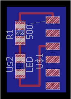
This week we learned how to design a PCB (Printed Circuit Board) with electronics design software. I used Eagle and the components from the fab library. Before redrawing the board for this week's assignment, I tried to create a simple circuit with a power source, an LED and a current-limiting resistor in the schematic view of Eagle. Then in the board view I added routing wire to complete the circuit. Here are the schematic and board views of the circuit and its traces:
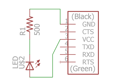

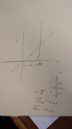
I asked Rob how to calculate the current through an LED and how we should determine which resistor to use. Here's the diagram he drew to illustrate how to calculate current:
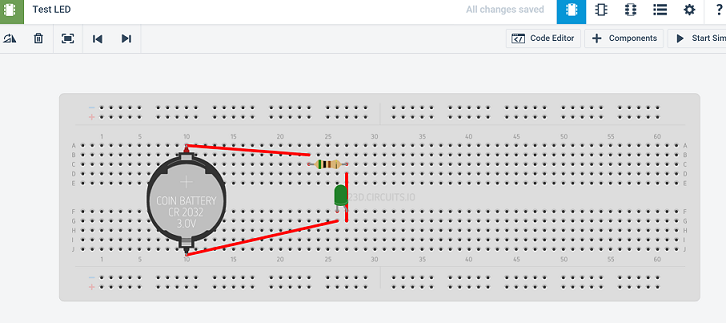
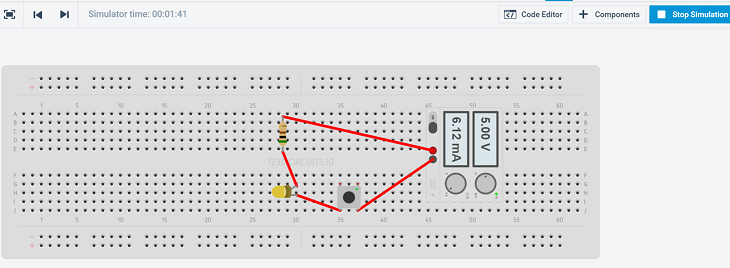
I also tried to use 123D to simulate this simple board.
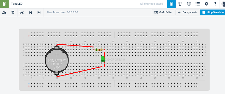
I then added a switch and simulated pressing the button to turn on the LED:
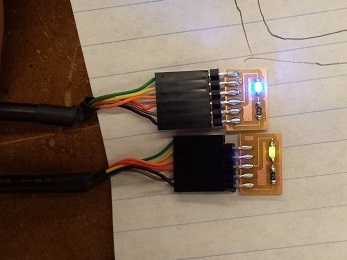
I made the actual board and the blue and lime green LEDs lit up:
This week we were supposed to recreate the echo hello-world board in a circuit design software, and add at least a button and an LED (with its current-limiting resistor). The original board looks like the following:
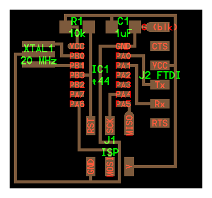
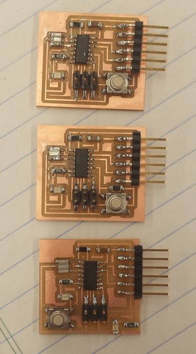
In order to recreate the board, I followed a tutorial that Rupal sent out. It was created by one of the students at the fab academy. I based my three board designs largely on this design, but made some modifications on two of the boards.
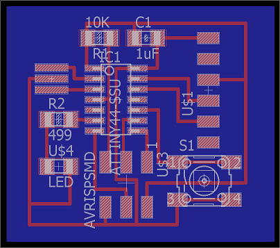
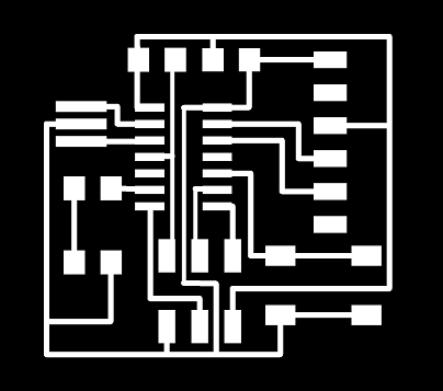
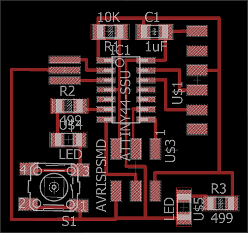
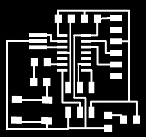
In my first attempt, I added a switch on the lower right-hand corner, and an LED and a resistor on the left-hand side. I did not add a resistor between the VCC (power source) and the switch. Here are the schematic view and the board view of the board, as well as the traces:

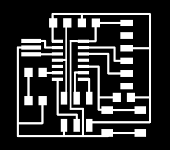
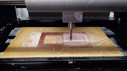
In order to fit the three vertical traces underneath the ATTINY44, I followed Albert's suggestion and changed the grid size from 0.05 (the default) to 0.005. Then I was able to move the lines with more flexibility and fit all three of them. When I imported the trace image into fab-modules for milling, I noticed that fab-modules could not read two of the three vertical traces underneath the ATTINY44 as separate lines and it clustered the two lines into one:
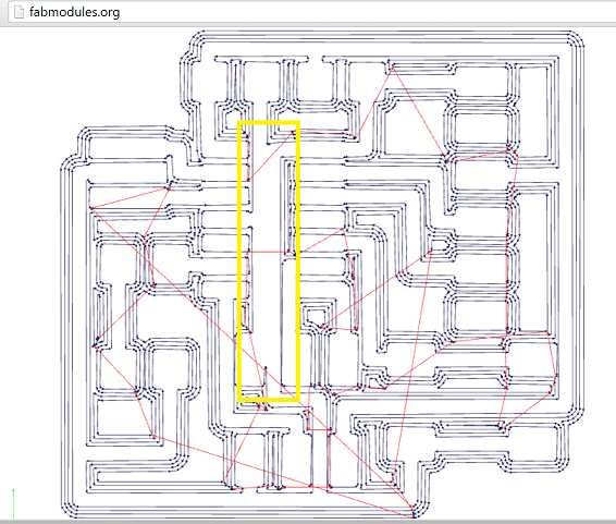
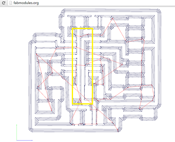
I tried moving those three lines further apart, but then one of the lines would cluster with the legs of the ATTINY44. I had to go back to the board view and change the width of the three routing wires from 0.016 (the default) to 0.012. To do this, in the board view, there's a "change" icon on the left-hand side panel. I clicked on "change...width (last option)" then changed the width to 0.012. Then I clicked on those three vertical traces. This action did not change the width of any other (unselected) wires. I almost couldn't tell the difference by eye, but fab-modules then was able to read the three traces as separate lines:
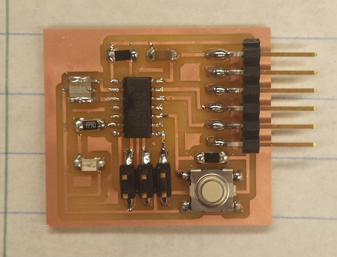
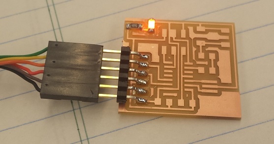
Then I went ahead to solder the board:
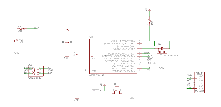
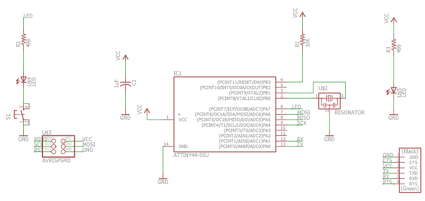
In my second attempt I added a resistor between the power source and the switch, recreating the same board as the one in the tutorial. The schematic and the board files are as attached.

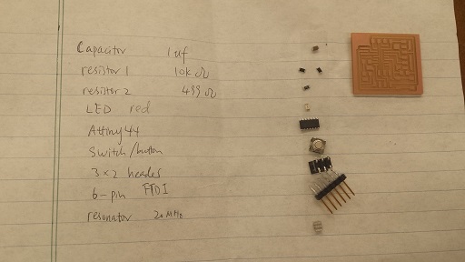
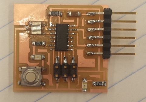
Here's the list of components and the actual board:
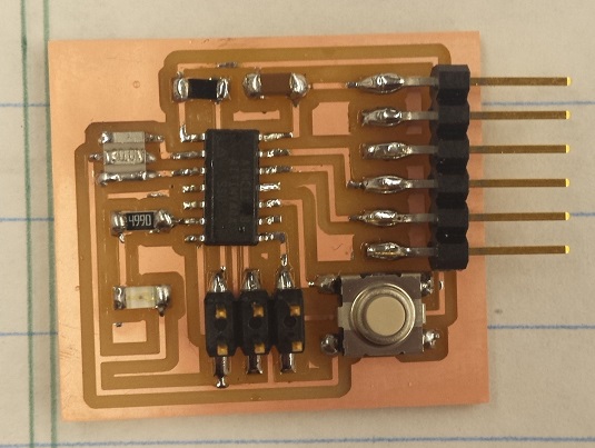
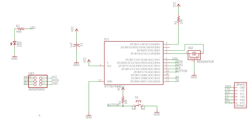
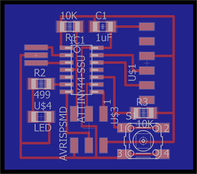
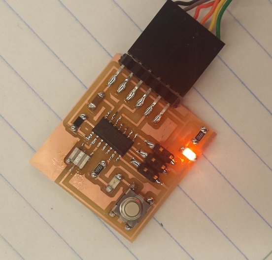
In my third attempt I added an LED between the VCC and the ground, and wanted to use that to make sure that the circuit was properly powered. I also placed the switch in series with another LED and its resistor. The schematic and board files are as attached.
I first soldered the LED and the 6-pin FTDI header and tested whether or not the LED would light up. After confirming that the LED worked, I soldered the rest of the board. Joe and Vincent showed me how to use a voltmeter to test for continuity to make sure that some components (especially the button switch and the 20 MHz resonator) were properly soldered.
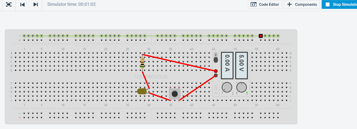
I did not simulate this board because I couldn't find the 14-pin ATTINY44 in 123D. The only ATTINY available in their components list was one with 8 pins. I will try to use another software to simulate these more complicated boards later. Here are the three boards I made this week: